CN
CN EN
EN


When the MOS switch is closed, the inductor converts the electric energy into the magnetic energy for storage
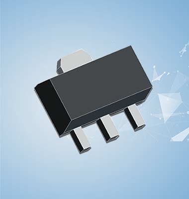
In the manufacturing process of depletion MOS FET, a large number of positive ions are added into the SiO2 insulating layer in advance. Therefore, when UGS = 0, the electric field generated by these positive ions can also "induce" enough electrons in the p-type substrate to form an n-type conductive channel. When UDS > 0, a larger drain current ID will be generated. If UGS is less than 0, it will weaken the electric field formed by positive ions, narrow the N channel and reduce the ID. When UGS is more negative and reaches a certain value, the channel disappears, id = 0. UGS with id = 0 is also called pinch off voltage, which is still expressed as up.
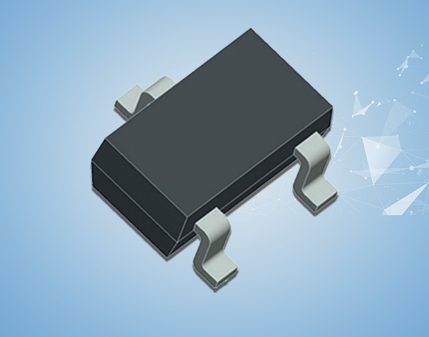
The structure of channel depleted MOSFET is similar to that of enhanced MOSFET, except that the channel already exists when the gate voltage UGS of n-channel depleted MOSFET is 0. The n-channel is pre fabricated on the surface of the substrate by ion implantation during the manufacturing process between D and s, which is called the initial channel.
When UGS = 0, the channel between drain and source already exists, so as long as UDS is added, ID will flow. If the forward gate voltage UGS is increased, the electric field between the gate and the substrate will induce more electrons in the channel, the channel will become thicker, and the channel conductivity will increase.